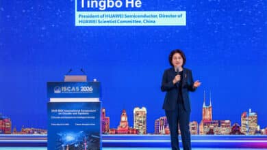
Huawei has introduced the Tau Scaling Law, positioning itself at the forefront of semiconductor innovation. Presented at the 2026 IEEE International Symposium on Circuits and Systems (ISCAS), this breakthrough offers a fresh direction for an industry facing the limits of Moore’s Law. By shifting focus from geometric to time-based advancements, Huawei aims to unlock higher transistor density and system performance.
How the Tau Scaling Law Reinvents Semiconductor Evolution
Moore’s Law has long guided semiconductor development, but recent years have revealed its limitations. Physical constraints and reduced economic returns have challenged the industry. The Tau Scaling Law proposes a new approach by replacing geometric scaling with time (τ) scaling. This principle encourages innovation by compressing signal propagation delay, thus advancing both transistor density and electronic system performance. The law offers a sustainable evolution path to meet growing computational demands.
Key Technologies: LogicFolding and System-Level Optimization
Huawei’s adoption of the Tau Scaling Law has led to several critical technologies and a coordinated design approach. Among the highlights:
- Device Level: Optimizing transistors and interconnects to minimize time constants and enhance physical efficiency.
- Circuit Level: Introducing the LogicFolding architecture to break traditional circuit boundaries, reducing critical-path wiring and boosting transistor density.
- Chip Level: Applying full-stack integration from software to silicon, resulting in more efficient data and instruction flows.
- System Level: Redefining protocols like UnifiedBus for improved memory and communication latency in high-performance computing environments.
These technologies work together to systematically increase overall performance, energy efficiency, and transistor density at every level.
Future Impact: Huawei’s Vision for Chips and Industry Collaboration
Over the past six years, Huawei has designed and mass-produced 381 chips based on the Tau Scaling Law. The upcoming Kirin chips, set to launch in fall 2026, will be the first to use the LogicFolding architecture, promising significant performance gains. By 2031, Huawei projects its high-end chips will achieve transistor densities similar to those of 1.4 nm processes. Looking to the future, Huawei emphasizes the importance of openness and collaboration, inviting global partners and experts to join in advancing semiconductor evolution.
In summary, the Huawei Tau Scaling Law introduces a time-based framework poised to surpass the limits of Moore’s Law. Backed by innovative technologies and a collaborative spirit, Huawei’s vision aims to ensure continued progress and sustainability for the semiconductor industry worldwide.
Don’t miss our latest Startup News: Bluon ServiceTitan Integration Delivers Powerful Boost to HVAC Pros