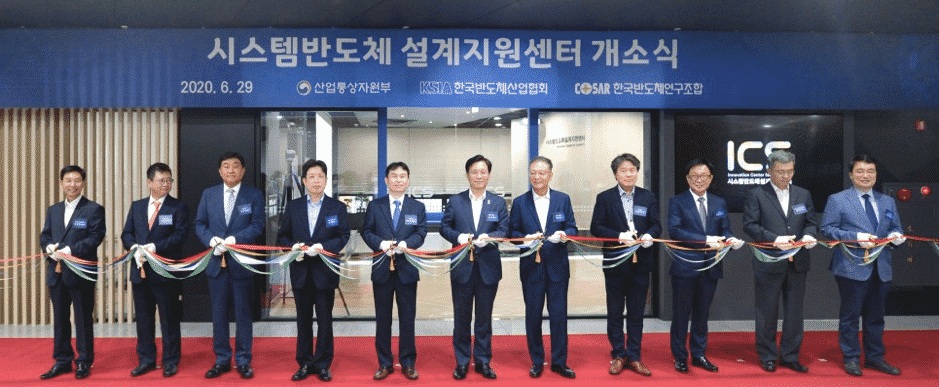
Now, you are one step closer to making your own semiconductor chip. Anyone who wants to design a semiconductor chip can really do it at this center that opens 24 hours, 365 days a year.
It is happening at the System Semiconductor Design Support Center. Chich recently opened at Gyeonggi Business Growth Center in Pangyo on June 29. At the opening ceremony, the Ministry of Trade, Industry and Energy (MOTIE) announced the new system semiconductor industry development strategy with the invited companies.
A vision and strategy for system semiconductor
The government had announced the vision and strategy for system semiconductor April 2019. The following step, System Semiconductor Design Support Center was opened to provide one-stop support for the development and commercialization of fabless companies.
The government plan to fund the cost to make the chips made by fabless at the foundry. In addition to this, it will also support commercialization and mass usage of the chips to expand the semiconductor IPs and made-in-Korea IPs.

MOTIE is currently selecting companies in nine industries including AI, touch-circuit, and autonomous vehicle sensors for fostering. It is planning to select 11 additional companies by 2021.
System Semiconductor Design Support Center is expected to strengthen the system semiconductor ecosystem. By providing an analysis and measurement infrastructure that evaluating the cost of implementing the designed chip as a prototype and whether the prototype is operating normally.
The government will also fully operate a system semiconductor fund of 100 billion won.
Minister Seong of MOTIE said. “We will strengthen the linkage between companies. So that Korea can leap into a system semiconductor powerhouse. And support industrial competitiveness by fostering professional manpower and supporting R&D.“


One Comment